| Item | Symbol | Conditions | Min. | Typ. | Max. | Unit |
| Operating supply voltage | VDD | - | 1.25 | 3.0 | 5.5 | V |
| Clock supply voltage | VCLK | - | 1.1 | 3.0 | 5.5 | V |
| Operating temperature | TOPR | - | -40 | +25 | +85 | °C |
| VDD detect voltage | -VDET2 | VDD,Fall | 1.20 | 1.30 | 1.40 | V |
| Item | Symbol | Conditions | Rating | Unit |
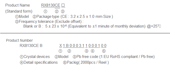
| Frequency tolerance | Δ f / f | Ta = +25 °C VDD = 3.0 V |
B : 5 ± 23* | x 10-6 |
| Oscillation start-up time | tSTA | VDD =2.75V to 5.5V | 1 Max. | s |
| Item | Symbol | Conditions | Min. | Typ. | Max. | Unit |
| Current consumption | IBK | SCL=SDA = "L" , VBAT=3.0V ,VDD=VIO=0.0V |
- | 300 | 500 | nA |
| V32K | SCL=SDA = "H" , FOUT=32.768kHz, /IRQ=OFF, VDD=VIO=3.0V, FOUT pin CL=15pF CHGEN=L or VBAT≧VDET3 |
- | 3.5 | 4.0 | µA |
| Signal Name | I / O | Function |
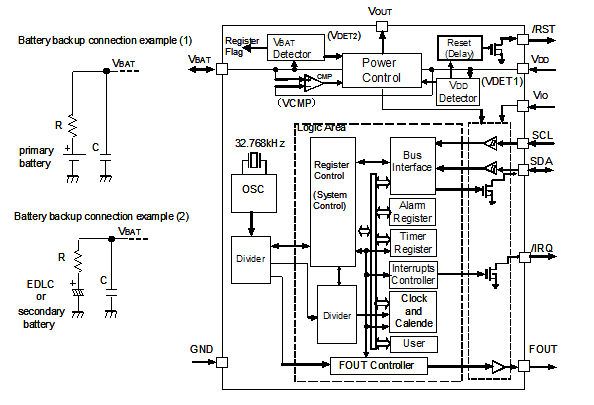
| SCL | input | Serial clock input pin. |
| SDA | Input / Output | Data input and output pin. |
| FOUT | Output | Frequency output pin with output control function. (C-MOS)Output frequency can be selected as 32.768kHz, 1024Hz, 1Hz. |
| / RST | Output | Reset output pin.(N-ch open drain) In case of VDD voltage drop detection, a reset signal is outputted. In case of VDD voltage rise detection, it is released reset signal after 60ms. |
| / IRQ | Output | Interrupts output by Alarm and Timer events.(N-ch open drain) |
| VDD | - | This is a power-supply pin. It can impress the voltage unlike VIO. |
| VIO | - | This is a interface power supply pin. This is a pin to supply the voltage same as a host. |
| Vout | - | Internal voltage output pin. Connect smoothing capacitor of 1.0µF |
| VBAT | - | This is a power supply pin for backup battery. This is a pin to connect a large-capacity capacitor, a secondary battery,a primary battery. In a backup power supply operating range, the voltage is supplied inside by this pin. |
| GND | - | Connected to a ground |
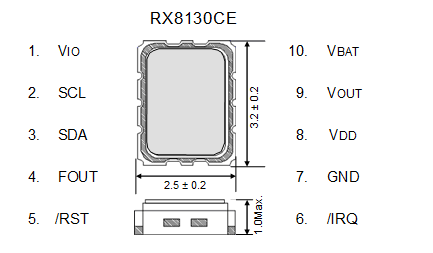
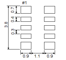
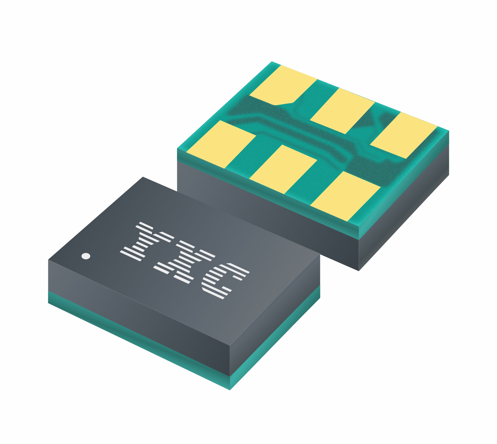
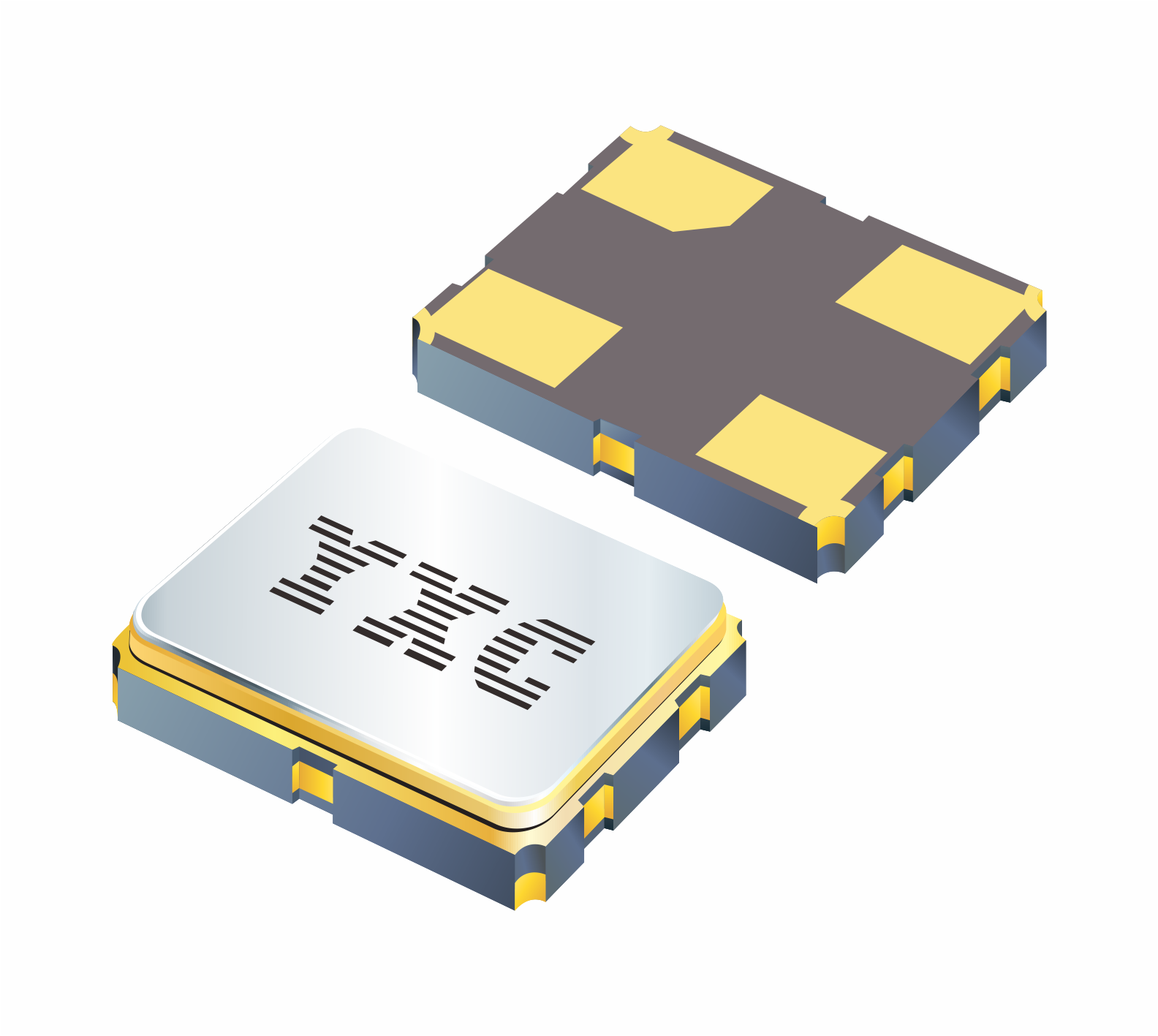
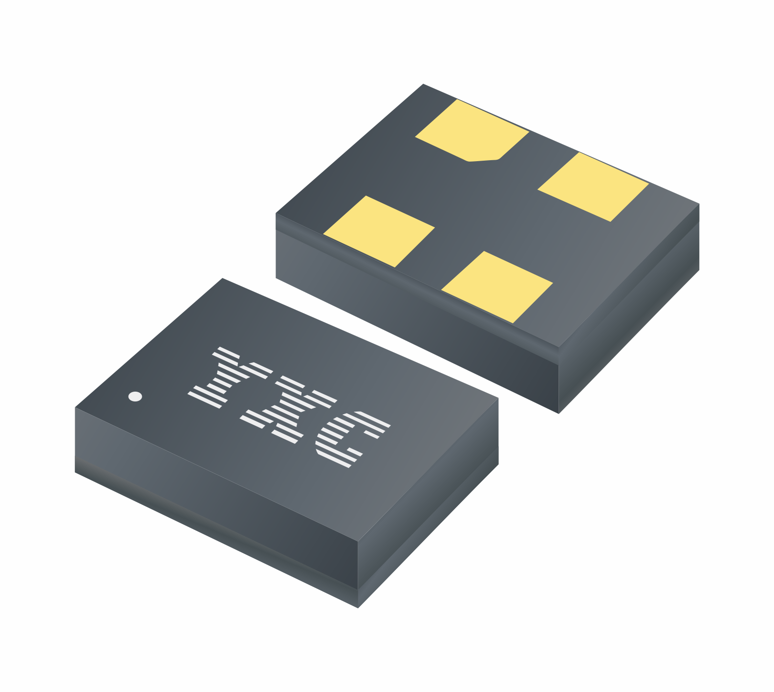
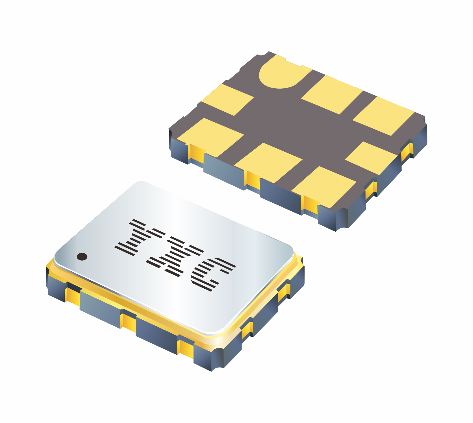
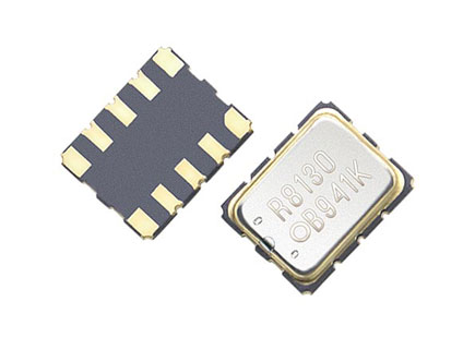
(Unit: mm)
To maintain stable operation, provide a 0.1uF by-pass capacitor
at a location as near as possible to the power source terminal of the crystal product (between Vcc - GND).
Voltage : 2.5V~5.5V
Frequency : 32.768KHz
Dimension : 3.2 x 2.5 mm
Operating Temp :
Frequency Tolerance : ±5ppm ±23ppm
Output : -