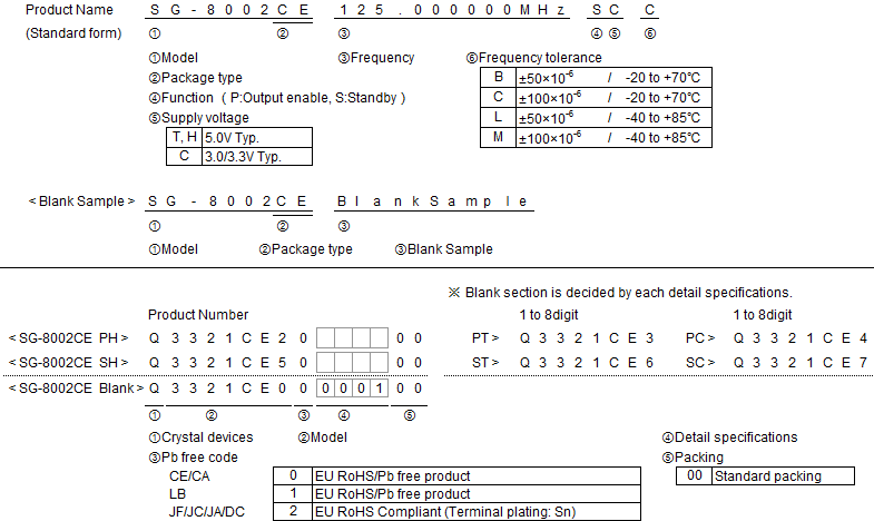
Rohs Status: Compliant
PN: Q3321CE40003200
Applications: Cellphone, Tablet, Health and Wellness Monitors Fitness watches, Sports Video Cams
| Item | Symbol | Specifications *2 | Condition/Remarks | ||
| PT / ST | PH / SH | PC / SC | |||
| Output frequency range | f0 | 1MHz to 125MHz | - | VCC =4.5V to 5.5V | |
| - | - | 1MHz to 125MHz | VCC =3.0V to 3.6V | ||
| - | - | 1MHz to 66.7MHz | VCC =2.7V to 3.6V | ||
| Supply voltage | VCC | 4.5V to 5.5V | 2.7V to 3.6V | ||
| Storage temperature |
T_stg | -55°C to +125°C | Store as bare product. | ||
| Operating temperature |
T_use | -20°C to +70°C / -40°C to +85°C | *1 | ||
| Frequency tolerance | f_tol | B: ±50 × 10-6, C: ±100 × 10-6 | -20°C to+70°C | ||
| M: ±100 × 10-6 | -40°C to+85°C *3 | ||||
| Current consumption |
ICC | 45mA Max. | 28mA Max. | No load condition, Max. frequency |
|
| Output disable current |
I_dis | 30mA Max. | 16mA Max. | OE=GND (PT,PH,PC) |
|
| Stand-by current | I_std | 50μA Max. | ST (ST,SH,SC) |
||
| Symmetry *1 | SYM | 40% to 60% | - | TTL load:1.4V, Max. load condition |
|
| - | 40% to 60% | CMOS load: 50% VCC level, Max. load condition |
|||
| 45% to 55% | *1 | ||||
| High output voltage | VOH | VCC -0.4V Min. | IOH=-16mA(PT,ST,PH,SH ), -8mA(PC,SC) |
||
| Low output voltage | VOL | 0.4V Max. | IOL=16mA (PT,ST,PH,SH), 8mA(PC,SC) |
||
| Output load condition (TTL) *1 |
L_TTL | 5TTL Max. | - | f0 ≤ 90MHzand Max. Supply voltage |
|
| Output load condition(CMOS) *1 |
L_CMOS | 15pF Max. | Max. frequency and Max. Supply voltage |
||
| Output enable / disable input voltage |
VIH | 2.0V Min. | 70% VCC Min. | OE terminal or ST | |
| VIL | 0.8V Max. | 20% VCC Max. | |||
| Rise / Fall time *1 | tr / tf | 4ns Max. | - | TTL load: 0.4V to 2.4V level |
|
| - | 3ns Max. | CMOS load: 20% VCC to 80% VCC level |
|||
| Start-up time | t_str | 10ms Max. | Time at minimum supply voltage to be 0s |
||
| Frequency aging | f_aging | ±5 × 10⁻⁶ / year Max. | +25°C, VCC=5.0V/3.3V (PC,SC) First year |
||
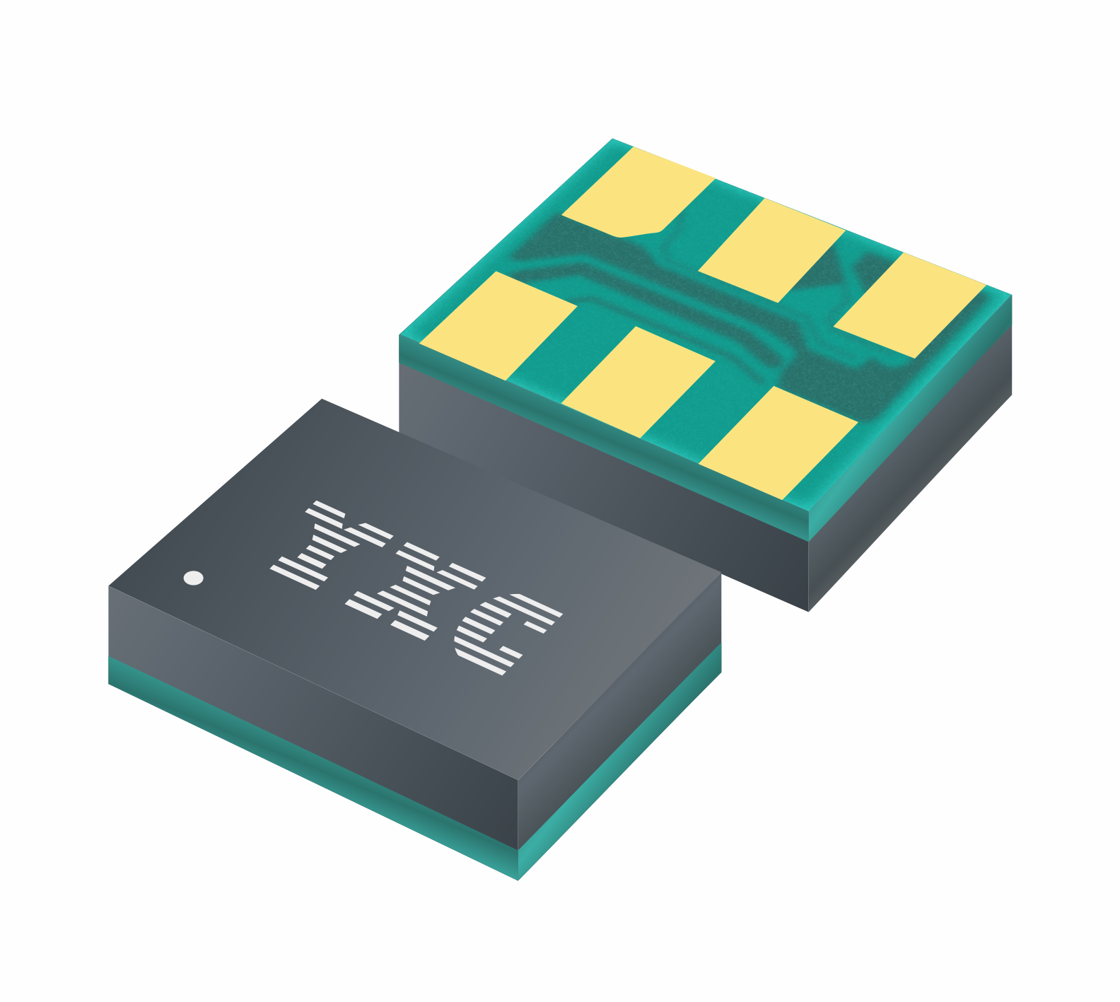
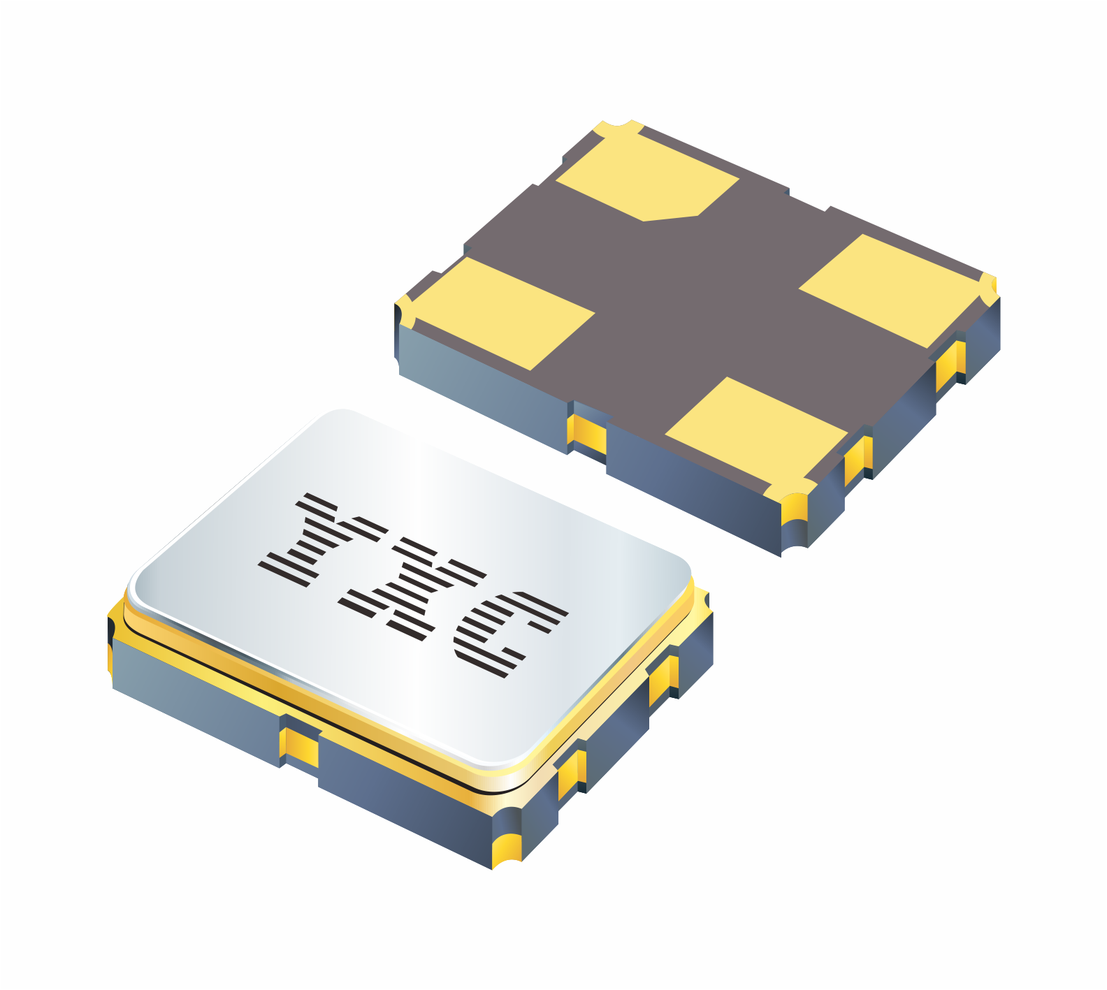
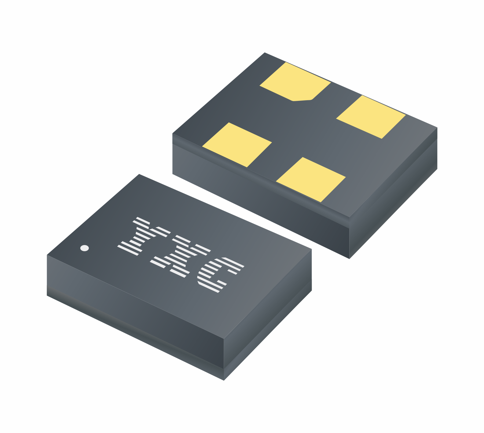
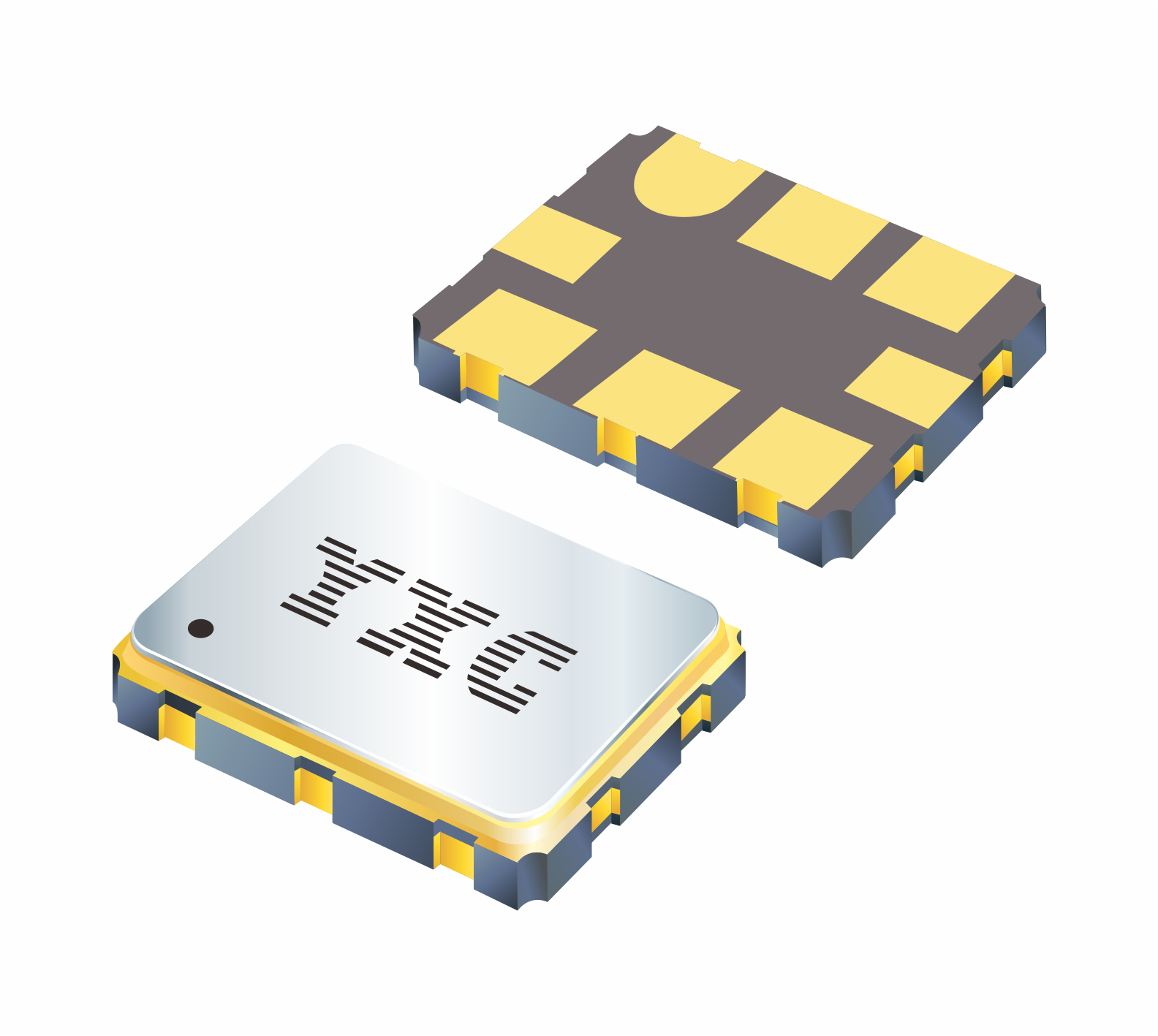
| Pin | Connection |
| 1 | OE or ST |
| 2 | GND |
| 3 | OUT |
| 4 | Vcc |
(Unit: mm)
Note.
OE Pin (PT, PH, PC)
OE Pin = "H" or "open": Specified frequency output.
OE Pin = "L": Output is high impedance.
ST Pin (ST, SH, SC)
ST Pin = "H" or "open": Specified frequency output.
ST Pin = "L": Output is low level (weak pull - down), oscillation stops.
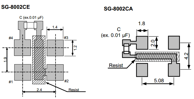
(Unit: mm)
To maintain stable operation, provide a 0.01 µF to 0.1 µF by-pass capacitor at a location as near as possible to the power source terminal of the crystal product (between VCC - GND).
Voltage : 2.7V~5.5V
Frequency : 1MHz-125MHz
Dimension : 2.5 x 2.0 mm 3.2 x 2.5 mm 5.0 x 3.2 mm 7.0 x 5.0 mm
Operating Temp :
Frequency Tolerance : ±50ppm ±100ppm
Output : CMOS