The RTC (Real-Time Clock) chip (model numbers YSN8900, YSN8025, YSN8010) is a specialized integrated circuit designed for precise timing and power failure continuation. Its core function is to provide stable timing measurements for seconds, minutes, hours, days, months, weeks, and years. Even after the main power supply fails, it continues timing operation using a backup battery without interruption. It is widely used in embedded systems, industrial control equipment, smart instruments, and consumer electronics.
Working Principle: The built-in crystal oscillator directly generates a stable 32.768 kHz base clock without requiring a load capacitor, completely eliminating issues related to crystal oscillator wiring, startup, and temperature drift. The temperature sensor continuously monitors the chip's ambient temperature and transmits the data to the temperature compensation unit. Based on a preset temperature-frequency compensation curve, the unit dynamically adjusts the output frequency to compensate for temperature-induced frequency drift, achieving ultra-high precision of ±3.4 ppm across the full temperature range of-40°C to +85°C. The compensated 32.768 kHz clock is then fed directly to the RTC Core as the timing reference.
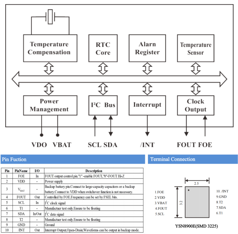
The core architecture consists of eight major functional modules: temperature compensation unit, RTC timing core, alarm register, temperature sensor, power management unit, I²C bus interface, interrupt control unit, and clock output unit. interconnected via an internal bus, all modules are powered uniformly by the power management unit and interact with the system through external pins.
RTC Timing Core Module:
The RTC Core serves as the functional hub of the RTC chip, fully integrated within the chip itself without requiring external circuits. It receives a temperature-compensated 32.768 kHz clock signal and, through an internal 15-stage division circuit, divides it into 1 Hz second pulses (32,768 kHz ÷ 2^15 = 1 Hz). These 1 Hz pulses drive the internal BCD code counting register, which increments automatically in the sequence "second → minute → hour → day → week → month → year," with automatic year correction without software intervention. The timing data is synchronized in real-time to the internal bus and can be read/write by the MCU via the I²C interface. It also interfaces with the Alarm Register to trigger alarms; when the elapsed time matches the preset value in the Alarm Register, an interrupt signal is generated and sent to the Interrupt unit. Additionally, it coordinates with the clock output unit to divide the timing clock into various frequencies (e.g., 32.768 kHz, 1 Hz, etc.), which are output through the FOUT pin.
Power Management Module: Power Failure Duration Guarantee (Corresponding Pins VDD/VBAT)
The chip features an integrated primary/backup power automatic switching circuit. When the primary power supply (VDD, typically 3.3 V) operates normally, the chip prioritizes using this power source. In the event of a primary power failure, the switching circuit seamlessly switches to VBAT (backup battery) power, with a typical backup current of only 0.55 μA at 3.0 V. Upon restoration of primary power, the system automatically returns to primary power supply without any interruption.
I²C communication interface module: Data bridge between MCU and RTC (corresponding to pins SCL/SDA)
Core Principle: Featuring a standard I²C two-wire interface, where SCL serves as the serial clock line (input clock provided by the MCU) and SDA as the serial data line (bidirectional data transmission/reception), supporting communication rates up to 400Kbps. Control commands are transmitted via the I²C bus to enable functions including reading time and temperature data, setting time and alarm parameters, configuring clock output frequency, and configuring interrupt modes.
Interrupt Control Module: Timed Wakeup and Alarm Reminder (Corresponding Pin / INT)
Core Principle: Receives trigger signals from the RTC core and alarm registers, configurable in various modes including alarm interrupt, second pulse interrupt, fixed-period timer interrupt, and time update interrupt. When the trigger condition is met, the /INT pin outputs a low level to wake up the sleep mode MCU, enabling low-power system design (e.g., scheduled wake-ups for industrial equipment or timestamp recording for fault alarms). The system supports interrupt output in standby battery mode, ensuring wake-up functionality even after power loss.
Clock output module: Programmable frequency output (corresponding to pins FOUT/FOE)
Core Principle: FOE is the output enable pin (input): a high level (1) enables FOUT output, while a low level (0) sets FOUT to a high-impedance state; FOUT is the clock output pin (output): its frequency can be configured via the internal FSEL bit register (e.g., 32.768 kHz, 1 Hz), derived from the RTC core clock through division; the output clock serves as a reference clock for other modules (e.g., the MCU low-power timer or external RTC calibration).