In many circuits, the system crystal oscillator clock frequency is very high, and the energy of the interference harmonics is also strong. In addition to being derived from the input and output lines, the harmonics will also radiate from space. This also leads to the fact that if the layout of the crystal oscillator in the PCB is not reasonable, it will easily cause a strong stray radiation problem, and once it occurs, it is difficult to solve it by other methods. Therefore, it is very important to layout the crystal oscillator and CLK signal line when laying out the PCB board.
· Equivalent circuit of crystal oscillator
In fact, the crystal oscillator acts like a series RLC circuit.
The equivalent circuit of the crystal oscillator shows a series RLC circuit, which represents the mechanical vibration of the crystal oscillator, and a capacitor in parallel represents the electrical connection with the crystal oscillator, and the crystal oscillator runs towards series resonance.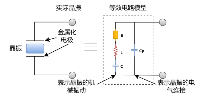
Among them, R is the ESR equivalent series resistance, L and C are the equivalent inductance and capacitance respectively, and Cp is the parasitic capacitance.
· Design layout of crystal oscillator on PCB board
As the heart of the digital circuit, the crystal oscillator affects the stability of the entire system. The choice of system crystal oscillator determines the success or failure of the digital circuit.
Since there is a quartz crystal inside the crystal oscillator, it is easy to cause the crystal oscillator to fail to oscillate due to external impacts and other situations. Therefore, when designing the circuit, it is usually necessary to consider the reliable installation of the crystal oscillator, and its location should be kept away from the edge of the board, the housing of the equipment, and other places. When laying out the crystal oscillator on the PCB, the following points should be paid attention to:
① The crystal oscillator cannot be too close to the edge of the board, and the shell of the crystal oscillator must be grounded, otherwise it is easy to cause the crystal oscillator to radiate noise.
This is especially important when designing the board. The grounding of the shell can prevent the crystal oscillator from radiating outward, and at the same time, it can shield the interference of external signals on the crystal oscillator. If it must be arranged at the edge of the PCB, you can lay another GND line on the edge of the crystal oscillator printed line, and at the same time, you can drill holes on the ground line at intervals to surround the crystal oscillator.
② The signal line cannot be laid under the crystal oscillator, otherwise it is easy to cause the signal line to couple the crystal oscillator harmonic noise.
Ensure that the ground is completely laid, and do not lay wires within 300mil of the crystal oscillator, so as to prevent the crystal oscillator from interfering with the performance of other wiring, components and layers.
③ If the filter device is placed under the crystal oscillator, and the filter capacitor and matching resistor are not arranged according to the signal flow direction, the filtering effect of the filter will be deteriorated.
The coupling capacitor should be as close to the power pin of the crystal oscillator as possible, and placed in descending order according to the power flow direction.
④ The routing of the clock signal should be as short as possible, with a larger line width, and a balance should be found between the wiring length and being away from the heat source.
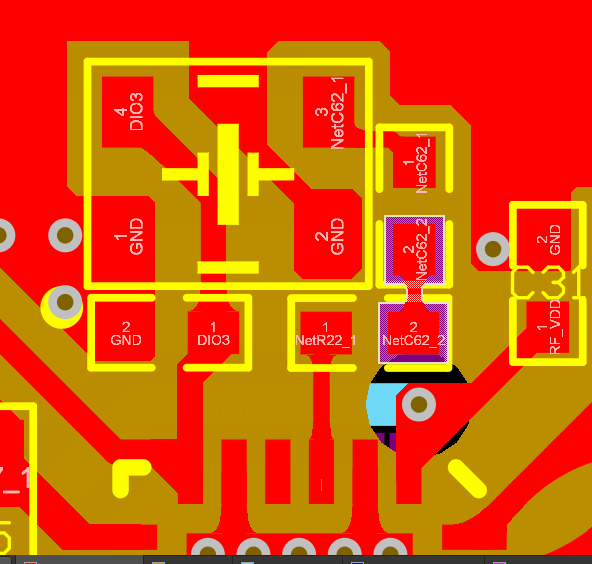
Taking the layout in the following figure as an example, the layout of the crystal oscillator will be relatively better:
① The filter capacitor and matching circuit of the crystal oscillator are close to the MCU chip position and away from the board edge.
② The filter capacitor and matching resistor of the crystal oscillator are arranged according to the signal flow direction, and are placed neatly and compactly near the crystal oscillator.
③ The crystal oscillator is placed close to the chip, and the routing to the chip is as short and straight as possible.
In the circuit system, the high-speed clock signal line has the highest priority. The clock line is a sensitive signal. The higher the frequency, the shorter the routing is required to ensure that the signal distortion is minimized.