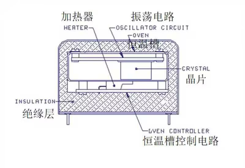
The oven-controlled crystal oscillator (OCXO) serves as the core component of high-precision frequency sources. It utilizes high-Q chips with optimized cutting profiles (e.g., SC-cut or AT-cut high-precision types) and minimal packaging stress. Through ultra-precise temperature control in an oven, the oscillator operates at the zero temperature coefficient point, effectively eliminating temperature-induced frequency drift. Widely applied in fields requiring extreme frequency accuracy, such as communications, navigation, and testing.
Understanding the pin definitions is fundamental to proper application of these components. The diagram shows the OCXO's package and pin layout.
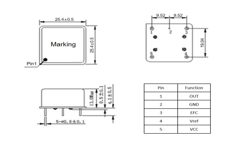
- OUT(Output):
Function: Frequency output pin, main signal output terminal
Common output types: Sine wave (for low-phase noise scenarios): Square wave (CMOS/LVCMOS, for digital systems)
- GND(Ground):
Function: It serves as the reference ground for all signals and power supplies.
Design considerations: single-point grounding, with short, thick, and straight grounding wires, avoiding sharing the ground with high-power current
- EFC(External Frequency Control)/VC(Voltage Control):
Function: Typically receives a DC control voltage ranging from 0 to +5V. By adjusting the capacitance of the varactor diode, it fine-tunes the crystal's resonant frequency, achieving a frequency pull range of ±0.1ppm to ±10ppm.
Typical voltage range: 0~5V
Typical frequency modulation range: ±1 ppm to ±5 ppm (some models can reach ±10 ppm)
Applications: Frequency calibration; Synchronous Phase-Locked Loop (PLL); Compensation for aging drift
- Vref(Reference Voltage):
Function: The OCXO internal voltage regulator circuit outputs a high-precision, low-noise reference voltage.
Typical values: 2.5V,3V,5V (specific values subject to manufacturer confirmation)
Application: Frequently used for fine-tuning bias in voltage-controlled VC (Voltage-Controlled) devices
characteristic :
Only output is allowed, not input (do not apply voltage to the Vref pin, as it may damage the internal reference).
Wait for the temperature to stabilize before powering on (the Vref value hasn't reached optimal precision until heating is fully complete).
If NC, it remains unconnected (neither grounded nor to VCC).
- VCC(Power Supply):
Function: To provide working voltage for the constant temperature chamber, oscillation circuit, buffer amplifier, and voltage stabilizing circuit inside the crystal oscillator.
Typical voltage: +3.3V, +5V, or +12V (depending on the model)
Characteristics: High heating current at startup (100~300mA), steady-state operating current of 50~150mA
Design note: Add a nearby decoupling capacitor (10μF + 0.1μF) to reduce ripple interference.
Common VC-OCXO Pin Errors and Troubleshooting
If the VC pin is connected as a power pin → The power supply voltage exceeds the voltage control range of the VC pin, directly damaging the internal varactor diode.
Long output line mismatch → Phase noise degradation, frequency hopping
Unfiltered power supply → Frequency modulated by power ripple
GND contact failure → complete stability failure
Using the device before ALM/RDY is ready → Significant frequency error
1. VCC Main Power Input (+3.3V/+5V/+12V)
2. GND Grounding Pin
3. EFC/VC voltage control input
4. Main frequency output
5. Vref (Reference Voltage) or NC (Not Connected)