As an indispensable signal transmitter in the clock circuit, the crystal oscillator is required for the microcontroller to operate normally. Therefore, the participation of the crystal oscillator is also indispensable in the design of electronic circuits. A good crystal oscillator circuit design can provide the best space utilization for electronics and play the greatest functional role.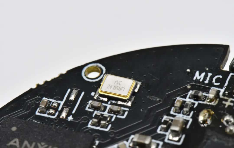
Crystal oscillator
Oscillation principle
The oscillator is a positive feedback amplifier with a frequency selection network without an input signal. From the energy point of view, the sine wave oscillator is a circuit that converts DC power into sinusoidal alternating energy of a specific frequency and amplitude by self-excitation. For any amplifier circuit with feedback, it can be drawn as shown in the figure below: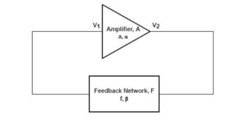
▲Figure 1 Oscillator
When the gain satisfies |f|×|a|≥1 and the phase condition satisfies α+β=2πn, a positive feedback loop is formed and the oscillation condition is met. The above figure constitutes an oscillator.
Crystal oscillator principle
When a certain alternating electric field is applied to both ends of the crystal, the chip will produce mechanical deformation. The quartz crystal oscillator is a resonant device made using the piezoelectric effect of the quartz crystal. If an electric field is applied to the two electrodes of the quartz crystal, the chip will produce mechanical deformation. At the same time, this mechanical deformation will generate a corresponding alternating voltage, and the amplitude at its characteristic frequency is much larger than the amplitude at other frequency points. According to this feature, in order to obtain a low starting voltage and a short starting time, the spectrum energy of the alternating voltage applied to both ends of the crystal should be mainly concentrated near the characteristic frequency of the crystal.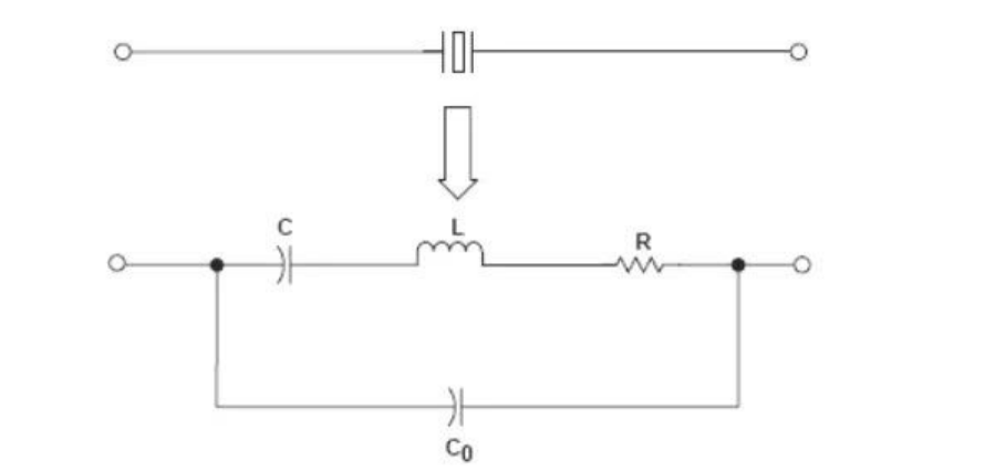
▲Figure 2 Crystal oscillator equivalent circuit
Under normal circumstances, the amplitude of the mechanical vibration of the chip and the amplitude of the alternating electric field are very small, but when the frequency of the applied alternating voltage is a certain value, the amplitude is significantly increased, much larger than the amplitude at other frequencies. This phenomenon is called piezoelectric resonance. The equivalent circuit of the quartz crystal oscillator is shown in Figure 2. When a parallel resonant circuit is formed with a quartz crystal, the crystal behaves as a sensor, and its equivalent quality factor Q value is very high. The equivalent impedance frequency characteristic is shown in Figure 3.
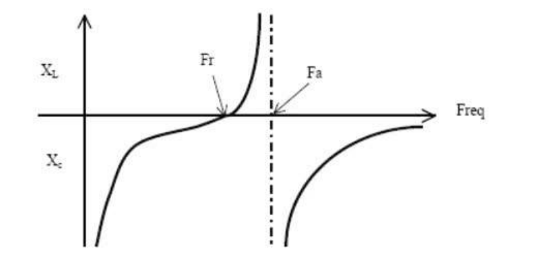
▲Figure 3 Crystal oscillator equivalent impedance
In Figure 3, Fr is the series resonance point. When the frequency is Fr = 1/(2π√LC), the series L and C in Figure 2 resonate, and the series branch is equivalent to a pure resistor. Fa is the parallel resonance point. At this time, the series branch is equivalent to an inductor, resonating with the parallel C0, Fa= Fr√1+C/C0. At this time, the equivalent impedance tends to infinity. Usually the difference between these two frequency points is very small.
In general, it can be considered that the crystal oscillator behaves as a resistor in series resonance and as an inductor in parallel resonance. It is recommended to use parallel resonance when designing.
In electrical engineering, this network has two resonance points, which are divided by the frequency. The lower frequency is series resonance and the higher frequency is parallel resonance.
Pierce oscillator
The inverter acts as an amplifier and provides a 180-degree phase shift at the same time. The crystal oscillator and negative resistance capacitor serve as feedback loops to provide the remaining 180-degree phase shift. RF is the feedback resistor, which is used to determine the DC operating point of the inverter so that it works in the high gain region (linear region). This resistance value cannot be too small, otherwise the loop will not oscillate. This circuit uses the parallel resonance of the crystal oscillator. Since the parallel resonance is related to C0 and will be affected by parasitic capacitance, increasing the load capacitors C1 and C2 can reduce the impact of C0 on the resonant frequency. At the same time, the addition of C1 and C2 will affect the start-up time and the accuracy of the oscillation frequency. The selection of load capacitors should be based on the values in the datasheet provided by the crystal oscillator supplier. Within the permitted range, the lower the load capacitance value, the better. Although a larger capacitance value is conducive to the stability of the oscillator, it will increase the start-up time.
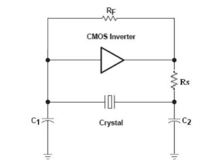
▲ Figure 4 Pierce oscillator circuit
Rs is used to suppress high-order harmonics, so that the oscillator obtains a purer spectrum. If the value of Rs is too small, it may cause overdrive of the crystal oscillator, resulting in damage to the crystal oscillator or shortened life. Usually Rs=XC2. The influence of Rs can be seen from the figure below.
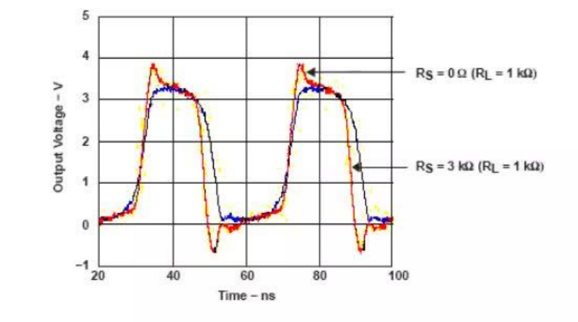
▲Figure 5 Influence of Rs (from references)
Circuit design
As shown in Figure 6, PM0 and NM0 form an inverter, which together with the off-chip circuit form an oscillation loop. PM7~PM9 and NM7~NM9 form a Schmitt trigger to shape and amplify the waveform. The output signal then passes through two stages of inverters to improve the output stage drive capability.
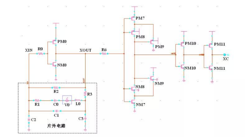
▲Figure 6 xtal circuit schematic
Simulation result demonstration
When Rs is small, under the same excitation voltage, the waveform amplitude is much smaller than when Rs is large, resulting in the XC output being a straight line.
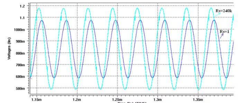
▲XOUT
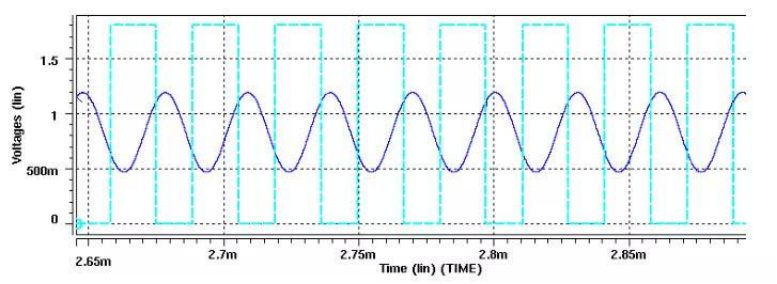
▲Figure 7 Waveform diagram of XOUT and XC
Crystal oscillator design precautions
The choice of crystal is very important in low-power design, especially for systems with sleep wake-up, which often use low voltage for low power consumption. Since the low power supply voltage reduces the excitation power provided to the crystal, the crystal starts oscillating very slowly or cannot start oscillating at all. This phenomenon is not particularly obvious during power-on reset. When the circuit is powered on, there is enough disturbance and it is easy to establish oscillation. When waking up from sleep, the disturbance of the circuit is much smaller than when powered on, and it becomes very difficult to start oscillation. In the oscillation circuit, the crystal cannot be over-driven (easy to oscillate to high harmonics) or under-driven (not easy to start oscillation).
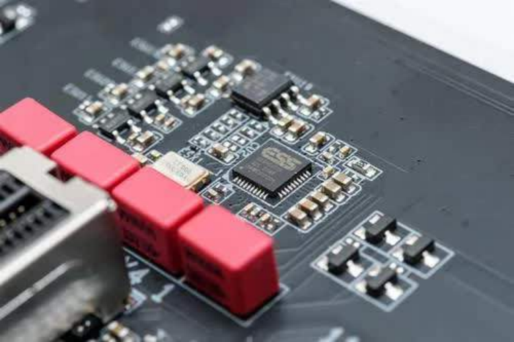
The selection of crystal should consider the following factors: resonant frequency, load capacitance, excitation power, temperature characteristics, and long-term stability. In other words, the reliability of crystal oscillator operation is not only affected by load capacitance. For the selection of load capacitance, it should be selected according to the value of the datasheet provided by the crystal oscillator supplier. Within the allowable range, the lower the load capacitance value, the better. Although a larger capacitance value is conducive to the stability of the oscillator, it will increase the start-up time. Some crystal oscillator recommended circuits even require a series resistor RS, which is generally used to prevent the crystal oscillator from being overdriven. Overdriving the crystal will gradually wear out and reduce the contact plating of the crystal, which will cause the frequency to rise, resulting in frequency deviation and accelerated aging.
Summary of design experience
01First, choose a crystal with low equivalent series resistance. Low crystal series resistance is conducive to solving the problem of starting oscillation. Because low crystal equivalent resistance is conducive to increasing loop gain.
02 Reduce the parasitic capacitance by shortening the connection spacing of the printed circuit board. This can help solve the problem of starting oscillation and the problem of crystal frequency stability.
03 The application temperature and voltage range of the crystal should be monitored to maintain the crystal starting frequency. If necessary, adjust the value of the capacitor and resistor.
04 For the best effect, the crystal design should use at least 40% of the peak-to-peak value of Vdd as the input signal to drive the clock inverter. This requirement cannot be achieved by simply adjusting the two ends of the crystal. We can also refer to the instructions of the crystal manufacturer for further help on crystal design.
05 The recommended optimal resistance value of R1 can be obtained by first calculating the values of capacitors C1 and C2, then setting a potentiometer at the position of R1 and setting the initial value of the potentiometer to XC1. In this way, the potentiometer can be adjusted to ensure that the crystal starts oscillating at the required frequency and maintains steady-state oscillation.